產品新訊
The new type of package technique makes MOSFET cooler than ever. With lower temperature as the advantage, the total resistance of the chip could become lower as well.
The resistance of MOSFET is mainly composed of the chip itself and package wire bonding. For practical application, lowering the resistance can lower the power consumption, heat and also increase the power transmission efficiency to extend the lifetime of MOSFET.
NIKO utilizes the PowerFET package technique shown in Fig. 1 and Fig. 2. To decrease the resistance induced by wire bonding, NIKO directly laminates the chip and package shell together, shown in Fig. 3. Simultaneously, the metal shell could also be the upper path of cooling and lower the surface temperature of MOSFET effectively, shown in Fig. 4.
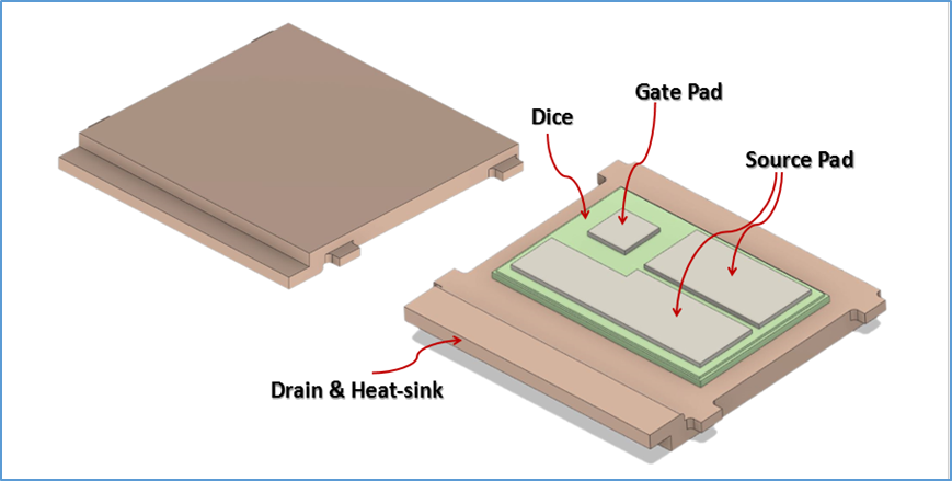 Fig. 1 PowerFET schematic diagram
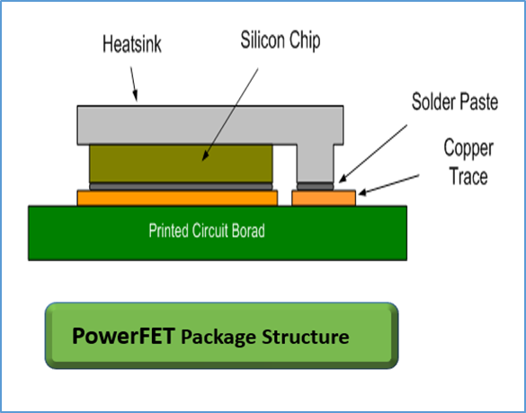 Fig. 2 PowerFET package structure
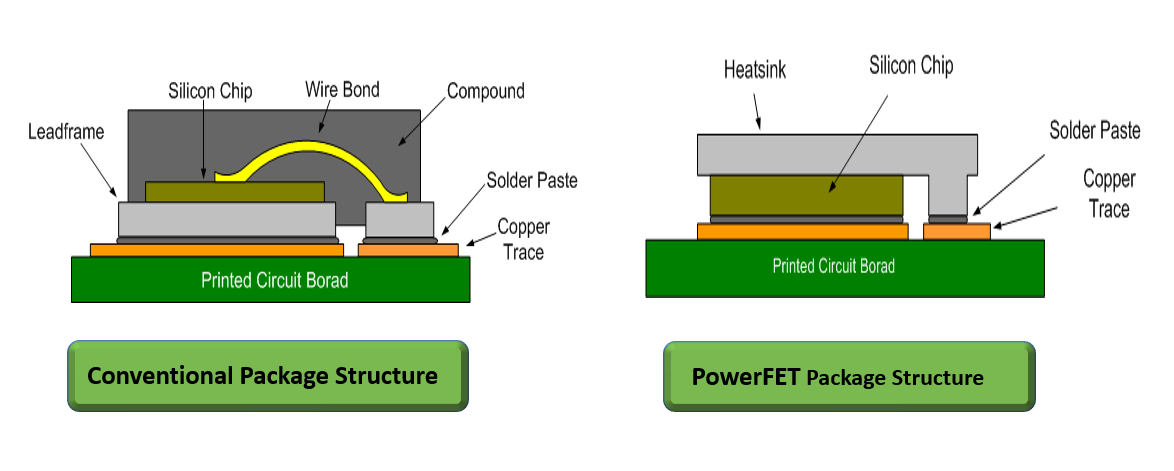 Fig. 3 Conventional package versus PowerFET package
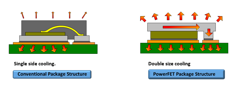 Fig. 4 The comparison of heat dissipation. The top metal shell act as heatsink in PowerFET.
NIKO combines the above advantages of new generation process and package technique together. The latest product which package size is 3mm X 3mm compares with the conventional DFN5x6 package, shown in Fig. 5 and the commonly used spec of the new PowerFET can be found in Table. 1.
Package type comparison
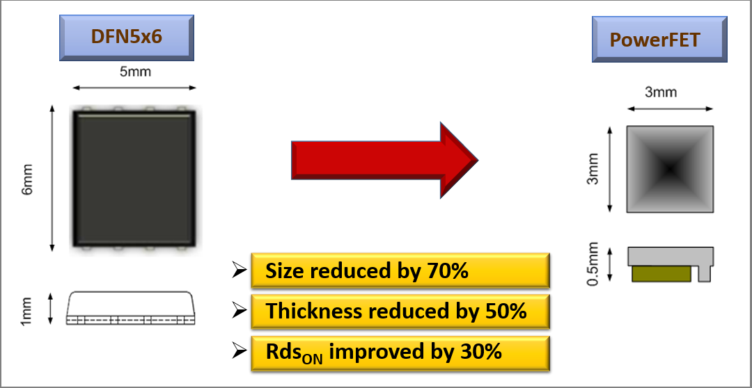 Fig. 5 DFN5x6 package versus PowerFET package
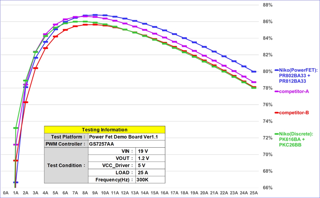 Fig. 6 The efficiency comparison in 19V/300KHz. PowerFET is apparently better than the conventional package (DFN5x6).
NIKO contributes to developing the new generation power device, PowerFET. PowerFET has an incredible cooling ability and extremely low conduction resistance. Furthermore, it also has a better power density. It could be used in many power kinds of application like DC-DC converter, load switch and the demand of future electronic system. In practical experiment of Buck converter, PowerFET has better ability of heat dissipation and high transmission efficiency, shown in Fig. 6. Confidentially, it is convinced that PowerFET will be all the rage in power society soon.
Select PowerFET for your application:


