Product News
A new structure for middle/low voltage optimizes or depresses ringing effect, shoot-through and switching loss.
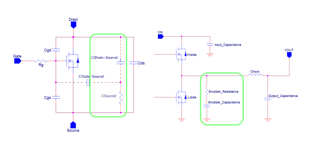
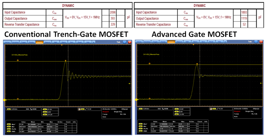
With this technique, the doping concentration in the drift area could be increased which makes the resistance in that area lower than the conventional trench-gate MOSFET. Simultaneously, due to the shielding effect, the breakdown voltage still can be kept in a great amount to prevent either punch-through nor reach-through. Moreover, there is a built-in snubber resulting from the new structure which can constrain the transient oscillation while turning on the device, shown in Fig. 1 and Fig. 2.
By comparison with conventional trench-gate MOSFET, the Advanced gate MOSFET has lower Q_RR and T_RR. With respect to this reason, the switching loss can be controlled exceedingly well. Lowering the total gate charge, especially the gate-to-drain charge, makes a big progress on improving the switching loss. Also, low ratio of Q_GD to Q_GS is a vital parameter of low side MOSFET to check the shoot-through immunity. If the ratio is much smaller than 1, it can be convinced that the synchronous buck circuit will not be easily disturbed inducing turn-on the MOSFET.
 Fig. 1 Built-in snubber schematic diagram
 Fig. 2 Practical waveform comparison between Conventional Trench-Gate MOSFET and Advanced Gate MOSFET
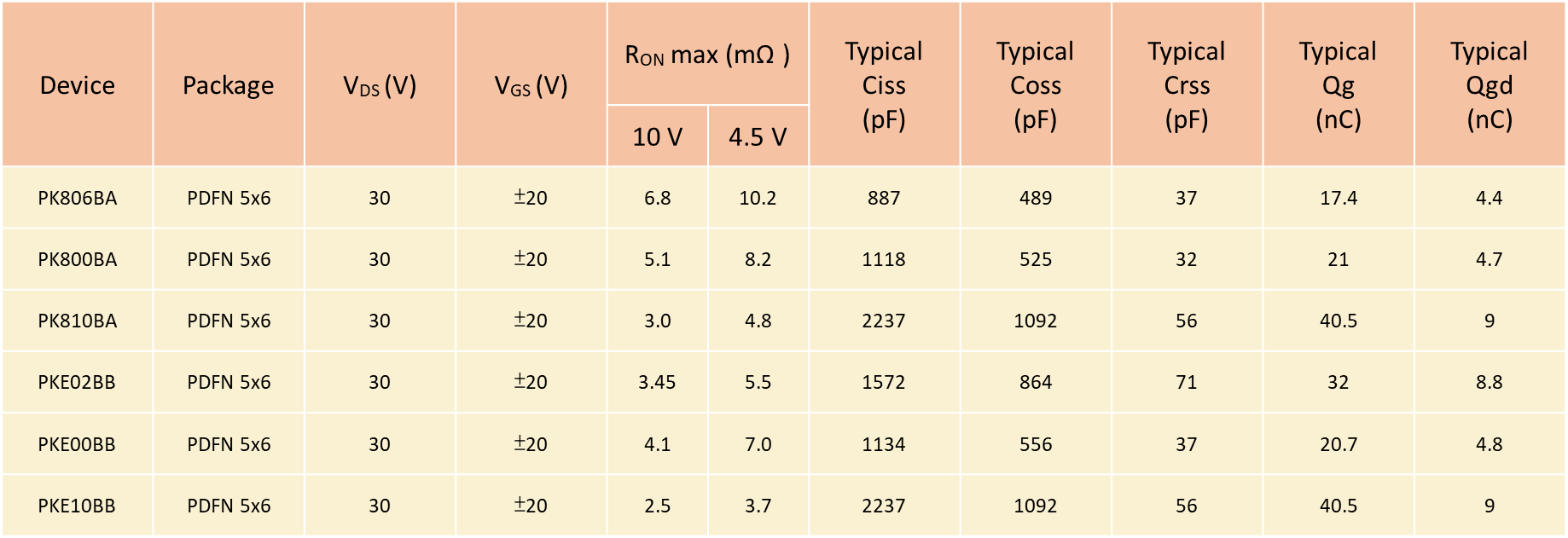
Select Advanced Gate MOSFET for your application:


